 Three HW building blocks were developed inside the WP4. Mainly exchanges occurred between end user and STM and Menta to provide requirements from the WP1 results. Some of them have been introduced in the modules before their prototyping in 2013.
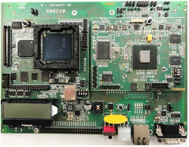
The three test vehicles have been manufactured and delivered for characterization purpose and potential improvement before their integration within the WP5 test vehicle.
ST test-vehicle prototyped two different configurable IPs on STM 65nm LP technology:
-
-
-
-
-
-
-
-
-
-
-
-
-
-
-
- CuBrick mask-programmable logic;
- PiCoGA, run-time programmable datapath.
Both the IPs have been evaluated for what is concerning the functionality and the performance, achieving results in line with expectation.
For the CuBrick mask-programmable solution, the activity confirmed the coherence and the alignment of all the CAD views with silicon results. On the design under verification, the IP reaches a working frequency of about 300MHz in nominal condition and a peak of about 350MHz over-driving the core-supply at 1.3V.
For the PiCoGA run-time programmable datapath, silicon prototyping confirmed the correctness of the CAD views with respect to both the functional specification and the timing characterization of the boundary annotated on the Liberty view. Concerning the performance evaluation, the working frequency of the device should be estimated about 100-150MHz on nominal conditions for mid-high complexity applications, while under highly-congested routing conditions the speed can slow down to about 50MHz.
No specific improvements have been required for the IPs, but a request to extend the programming flow of PiCoGA has been considered useful to overcome the area limitation of the WP5 test-vehicle. For that, PiCoGA programming flow has been improved adding an emulation model to allow synthesizing the code on standard FPGA.
PiCoGA emulation model is intended as a simple and quick way to emulate/simulate PiCoGA without the overhead of managing the bitstream-accurate model. This can allow designers to verify the system integration of the PiCoGA Interface with less computational requirements or to prototype the system on third-party FPGAs, moreover PiCoGA emulation model is much lighter in terms of complexity and it does not require any change on the PiCoGA Interface, which is the same for emulation and hard-macro integration.
The next figure shows the basic concept of the PiCoGA emulation model. Starting from the Griffy-C description of the PiCoGA operations, the same tool which generates the bitstream also provides a behavioural VHDL model. This model shall be compiled with the standard PiCoGA Interface and the emulation library of native Griffy-C operators. The resulting design can be used for both simulation and synthesis on third-party FPGA devices.
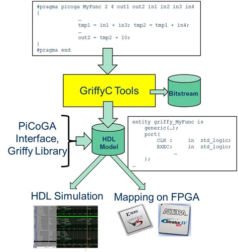
The model has been verified on HDL simulator using test-cases pre-verified on the hardware device, thus ensuring the functionality and the correspondence of the boundary signals with respect to the hardware device.
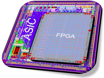
One of the major results is the eFPGA physical implementation on STM CMOS065LP silicon process and it covers:
- The eFPGA specification;
- Implementation of different basic blocks: eLBs, DSP and embedded memory block;
- The custom cells designed for CMOS065LP process to improve area density;
- The specific floorplan technique due to regular structure;
- The verifications done;
After the manufacturing step by STM, a PCB was specifically designed and manufactured to evaluate and characterize eFPGA test-vehicle. Menta realized a completed verification including functional verification and associated performances. Results are the following:
- All basic blocks like eLB, DSP and embedded memories are functional;
- Custom blocks like the memory bit cell and multiplexer are correct;
- The bitstream sending and reading during operations is also validated;
- The correlation between Menta programming software and hardware is correct because all mapped applications tested were correctly achieved on eFPGA.
The eFPGA implementation was constraint to 100 MHz maximum frequency for bitstream sending and reading and also for application. All measures give result at least 100MHz of maximum frequency so both timing and power performances are in line with implementation.
For more information about this Work Package please contact the Project Leader.

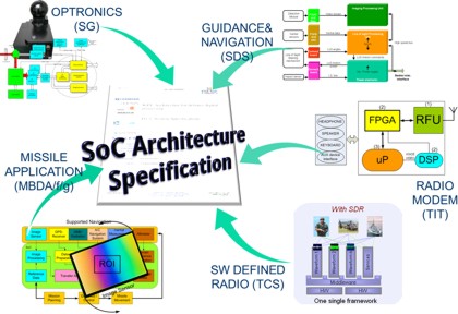 First activity of the WP1 was to collect system requirements for the various targeted product. This has been done covering the following applications:
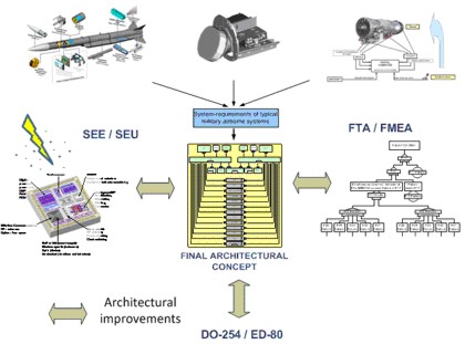
 To cover the initials objectives the partners have specified the requirements of the test chip and have selected one of the HW building blocks developed within the WP4. Embedded FPGA has been selected for the CORSAIR test chip.